
Papan HDI umumnya diproduksi menggunakan metode laminasi. Semakin banyak laminasi, semakin tinggi tingkat teknis dewan. Papan HDI biasa pada dasarnya dilaminasi satu kali. HDI tingkat tinggi mengadopsi dua atau lebih teknologi berlapis. Pada saat yang sama, teknologi PCB canggih seperti lubang bertumpuk, lubang listrik, dan pengeboran laser langsung digunakan. Berikut ini adalah sekitar 8 lapisan robot HDI PCB terkait, saya berharap dapat membantu Anda lebih memahami robot HDI PCB.
Quick Details of Robot HDI PCB
Place of Origin:Guangdong, China
Brand Name:Robot HDI PCB Model Number:Rigid-PCB
Base Material:ShengYi
Copper Thickness:2oz Board Thickness:1.2mm
Min. Hole Size:0.2mm Min. Line Width:4mil Min. Line Spacing:4mil
Surface Finishing:ENIG
Number of layers:8L PCB Standard:IPC-A-600
Solder Mask:Black
Legend:White
Product quotation:Within 2 Hours
Service:24Hours technical services Sample delivery:Within 10 days
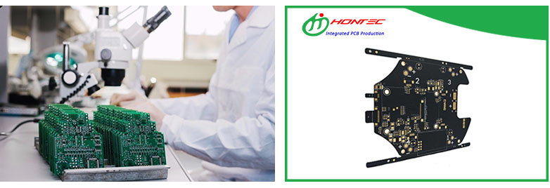
HONTEC Quick Electronics Limited (HONTEC), established in 2009, is one of leading quickturn Printed Circuit Board manufacturer, who specializes in high-mix, low volume and quickturn prototype PCB for high-tech industries in 28 countries. Upon efficiently quick around operation, PCB products contain 4 to 48 layers, HDI, Heavy Copper, Rigid-Flex, high frequency microwave,and Embedded Capacitance, and provides "PCB One-stop Shop" service to meet customers’ diverse demands. HONTEC is capable of producing 4,500 varieties monthly to meet 24-hour delivery for 4 layers PCB, 48-hour for 6 layers and 72-hour for 8 or more high-layer PCB at the fastest. Located in SiHui of GuangDong,HONTEC partners up with UPS, DHL and world-class forwarders to provide efficient shipping services.